38-32, 5-chome, Minami-cho, Fuchu-shi, Tokyo, Japan
MINAMI Co., Ltd. headquater
MINAMI Co., Ltd. headquater
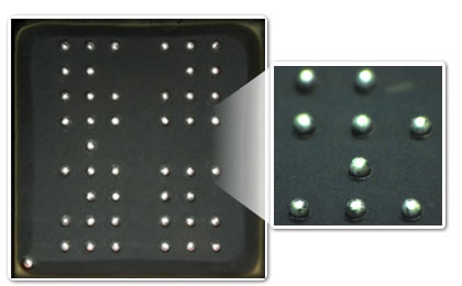
Solder bump printing onto WLCSP (wafer level CSP)【Pattent】
■ Outline
- Rewiring on wafer by a pressurized screen printer
- Plane printing with hole shaped openings and isolated land shape printing
(1). Insulation film forming on a wafer
(2). Polyimide passivation film formation by printing
(3). Plane printing with hole shaped opening and isolated land shape printing of Polyimide passivation film - Solder bump forming by pressurized and rotary squeegee printing

- Process

- Product image
- Cross section photograph

Copyright© 2013 MINAMI Co.,Ltd. All rights reserved.